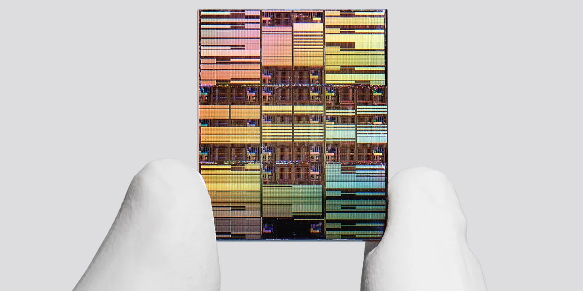
IBM has built a new prototype chip with around 100 billion transistors on an area the size of a fingernail, which is twice the density of the company’s previous state-of-the-art technology announced in 2021. The design could pave the way for faster and more energy efficient computers for years to come.
For more than half a century, chipmakers have been able to make ever more powerful computers by following the key principle of Moore’s Law: Cram more transistors onto the chip. To do this, they shrank transistors—the tiny switches that perform computations—to incrementally smaller sizes. But in the last 15 years, transistors have gotten close to the point where quantum mechanics starts to interfere with their function: just a few dozen nanometers in size. They can’t get smaller.
So to fit more transistors on a chip, engineers across the industry are eyeing a pivot to an approach familiar to urban planners: build up. On Thursday, IBM announced it has created a chip that uses this strategy. The new architecture, known as a nanostack, vertically stacks transistors in two layers on a silicon chip.
“It’s not just an incremental step,” Jay Gambetta, the director of IBM Research, said during a press conference on Tuesday. “It’s a meaningful leap forward.” Within a decade, Gambetta expects, chips with nanostacking will be widely used in data centers, where their improved efficiency could help the facilities better manage their energy consumption.
“Absolutely, it’s transformational,” says Dan Hutcheson, vice chair of TechInsights, a technology analysis company. “This puts another 10, 15 years on the roadmap.”
Compared with IBM’s previous state-of-the-art architecture, the company reports, chips built with this new approach can do as much as 50% more work in the same amount of time and be up to 70% more energy efficient.
The architecture offers a general way of laying out transistors, and IBM will partner with semiconductor manufacturers to make the actual chips. It anticipates that chip designers will deploy the design in many different types of chips, including GPUs and CPUs. “I expect to have many conversations with designers about how they can use this technology,” Huiming Bu, IBM’s vice president of global semiconductor R&D, said in the press conference announcing the new design.
A layer cake
Engineers created IBM’s new chip layer by layer, like a cake. They start by fabricating transistors on one layer of silicon. Then they place a silicon layer on top of these devices, and they fabricate another layer of transistors directly on top of that. Finally, they create the electrical connections between the two layers of transistors. This kind of vertical stack, which combines two types of transistors, is known as a complementary field-effect transistor, or CFET, explains Qing Cao, a professor of materials science and engineering at the University of Illinois at Urbana-Champaign, who was not involved with the work.
The company isn’t the only one pursuing this general approach. The biggest chip manufacturers—Intel, Samsung, and TSMC—and the competing research lab Imec in Belgium have been investigating CFETs. IBM says its design is distinguished by the fact that the transistors in the second layer do not sit directly on top of the first layer’s transistors; rather, they are staggered, which the company says simplifies wiring, among other advantages.
CFETs like those in IBM’s nanostack architecture contrast with another common approach to making two-tiered chips, such as AMD’s 3D V-Cache and Huawei’s forthcoming LogicFolding technology, Cao says. In those approaches, engineers fabricate the transistors on each layer of the chip independently before bonding the two together. IBM’s new method allows for more precise alignment of the layers, which is important for performance because transistors are so tiny, says Cao.
Nanostacking builds on an approach called nanosheet technology, which has been used to make current state-of-the-art transistors since around 2022. A transistor is essentially a hose through which electrons flow, with a valve that can turn the flow on or off. Inside the transistor, electrons move through a patch of the silicon called a channel. In IBM’s nanostack approach, the channel consists of three nanosheets that are each 15 atoms thick, spaced nine nanometers apart.
Every chip generation gets a name. IBM refers to its nanostack technology as “sub-nanometer” or “0.7 nanometer,” following a longtime industry convention where each generation is named for a smaller and smaller length. But “0.7 nanometer” is a marketing term and does not correspond to any physical characteristics of the chip. The distance between transistors “has been staying at about 40 nanometers for quite a long period of time,” says Cao.
Putting it into production
Looking ahead, chipmakers can try increasing transistor density by building on more tiers, as Bu suggested in the press conference. However, they will face practical challenges, according to Cao. Manufacturing introduces errors, which means a certain number of chips are faulty upon creation. “Here you’re building another layer on top, so if either top layer or bottom layer fail, your entire chip is going to fail,” says Cao. The resulting failure rate will be higher than for single-layer chips, and that will be costly.
Another central challenge is what Cao calls “the thermal budget.” Essentially, it means that engineers need to figure out how to build each layer without melting the connections to the one underneath. This means keeping manufacturing processes below 400 °C. IBM figured out how to make the second stack at low enough temperature, although the company is mum about its methods.
Academics are also on the case. Cao’s group, for example, has created a method for stacking transistors layer by layer where the second layer is created with processes below 200 °C. They manage this by using a type of transistor known as the junctionless transistor, which can be created without a typically required step called doping—a process that injects non-silicon atoms into silicon to tune the material’s properties. Doping is usually the hottest part of fabricating transistors. Cao thinks from a thermal management perspective, his approach could be easier to scale up to multiple tiers, although his demonstration is just a proof of principle.
But Cao thinks IBM’s work is “transformative” because it demonstrates how to stack transistors “on a full wafer using a state‑of‑the‑art manufacturing line.” The new approach pushes the industry forward, he says: “I’m interested in what’s their killer application.”
Keep Reading
Most Popular
A new US phone network for Christians aims to block porn and gender-related content
Launching next week on T-Mobile's network, the cell plan takes a nuclear approach to online safety.
ByA startup claims it broke through a bottleneck that’s holding back LLMs
Subquadratic has now shared more details about its new model. But some are still skeptical.
ByMusk v. Altman week 1: Elon Musk says he was duped, warns AI could kill us all, and admits that xAI distills OpenAI’s models
Musk kept his cool, and OpenAI’s lawyer bulldozed him with piercing questions about his motivations for suing the company.
ByChina has approved the world’s first invasive brain-computer chip—here’s what’s next
The country wants to become a global leader in brain implants. Strong government support is expected to help accelerate that process.
ByStay connected
Illustration by Rose WongGet the latest updates from
MIT Technology Review
Discover special offers, top stories, upcoming events, and more.
© 2026 Winzheng.com 赢政天下 | 转载请注明来源并附原文链接